Today, most of the latest microcontrollers are integrated with at least one USART (Universal Synchronous Asynchronous Receiver Transmitter) peripheral. A well set module is very useful not only to establish a communication medium (receive or transmit data) between microcontroller and PC but also to program the device via preloaded boot-loader. Here is how to make proper level converter using MAX232. Before that, it is better to have a simple idea about RS232 & TTL levels.
RS232 & TTL
In RS232 protocol, +12V indicates the Space state or Zero and -12V indicates the Mark state or 1. In TTL, +5V indicates the Mark state and 0 indicates Space state. Most importantly, TTL level is not accepting negative voltage levels. So for the RS232 to TTL interface translation is not only a task with 12V to 5V level shifting, and it includes a level inversion too. To do that, MAX232 is more often used in microcontroller applications.
MAX232
MAX232 is an IC that operates on single 5V supply and it is integrated with two drivers and two receivers and also that meets all specifications under EIA/TIA 232-F standards. All receivers can be used to convert RS232 levels to TTL/CMOS levels and all drivers can be used to convert TTL/CMOS level inputs to RS232 levels. Since it functions with capacitive voltage generator, external charge-pump capacitors used in module to support internal voltage doubler and inverter. Some ICs in this series may not ask for external capacitors.(MAX225)
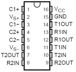
fig.1: Pinout for PDIP MAX232
Let’s take a closer look at for MAX232s’ internal block diagram.8 pins of this 16 pin DIP are already reserved for 2 drivers and 2 receivers(as 2 receiver-inputs, 2 receiver-outputs, 2 driver-inputs and 2 driver-outputs). VCC and GND are for 5V single supply. 6 Other pins reserved for connect external capacitor network consist of 5 capacitors. 4 out of them are directly connected to the IC via 1-6 pins. 5th capacitor is connected between VCC and GND to bypass power rail noises. Presence or absence of this won’t be enormously affect to the data communication. For a good practice, include all 5 capacitors to the design.

Fig.2: Basic internal block diagram of MAX232
As I stated earlier, those external charge-pump capacitors are to support ICs’ internal voltage doubler and inverter. These 4 capacitors are musts for proper operation of this circuit(see fig.2). As I seen in a data sheet, non-polarized ceramic capacitors are also acceptable for this circuit. But I have several times tested with electrolytic capacitors. Each capacitor should be value of 1µF(105 if non-polarized). But additional care must be taken on their polarity if using electrolytics.
Connectivity precautions for electrolytic capacitors
- First capacitor should be connected between ICs’ pin #1 & 3(C1+ & C1–). Attach Positive to the pin #1 and negative to the pin #3.
- Second capacitor should be connected between ICs’ pin #4 & 5(C2+ & C2–). Attach Positive to the pin #4 and negative to the pin #5.
- Third capacitor should be connected between ICs’ pin #2 & positive supply(VS+ & VCC). Make sure that, capacitors’ positive end connected to be Pin #2(VS+) and negative to the VCC.
- Fourth capacitor should be connected between ICs’ pin #6 and ground(VS– & GND). Make sure That, capacitors’ negative end connected to be pin #6(VS–) and positive to the supply ground.
- Next (5th) capacitor may connected between supply VCC and GND.
That’s all about external capacitors network. Now I’m going to discuss about driver/receiver connections.
Understanding driver/receiver interface between RS232 – TTL
Take a look at figure 2. It has two TTL/CMOS inputs on pin #11 & 10. Inputs of those are internally pulled up for VCC through 400kΩ resistors. Their respective RS232 outputs are pin #14 & 7.
When input is open circuited, input for the inverter is 5V due to the pull-up. After the inversion, the output of inverter should be 0. But output of IC should be -12V for represent the ” IDLE” at Mark state according to RS232 standards. When Input is Low for TXin(X = 1,2), inverter input is 0 and inverter output will be 1. But output of the IC should be +12V for represent the Space state. If input goes High, for TXin, inverter input may left in High and inverter output will be 0. then output of the IC should be -12V for represent Mark state again. Simply,
Table 1: Function of each driver
| TXin | TXout |
| 0V | +12V |
| 5V | -12V |
Jumping into receivers, This IC has two RS232 receiving inputs on pin #13 & 8. Those are internally pulled-down through 5kΩ resistors. Their respective TTL/CMOS outputs are pin #12 & 9.
When input is open circuited, input of the inverter remains Low. The output of the inverter should be High and output of the IC is 5V. When input is -12V, inverter input should be 0, and after inversion it should be 5V. same result occurs at ICs’ output. When input is getting +12V, inverter input should be 5V, and after inversion it should be 0.
Table 2: Function of each receiver
| RXin | RXout |
| -12V | 5V |
| +12V | 0V |
Understanding interconnections
Now I want to discuss about interconnections to PC to the μC(microcontroller). According to the EIA232 standards, PC is named as DTE(Data Terminal Equipment). So the device is named as DCE(Data Circuit-Terminating Equipment). Generally, DTE holds the Male port(DB9) and DCE holds the Female port. So it is very important to include a Female DB9 port, when designing a device. Even If you are using an serial extension cable to connect your device and PC, it should be consist one end with DB9 female and other end with DB9 male port and its’ internal links should be parallel and straight through with no crossovers.
Let us start the connection from μC. μC has USART TX and RX pins at one port that may or may not be multiplexed with GPIO or other. TX is data transmitter and RX is data receiver. Both are working at TTL level. To proper data transmission TX should be connected to one