I2C is a communication protocol developed by NXP semiconductors for communication between devices within a short distance. In I2C protocol master slave relationship exists between devices and slaves contains I2C address for each of them.Sensors such as MPU6050 or ADXL345 has the same I2C address for all of them. So it is difficult to use more than one MPU6050/ADXL345 sensor with I2C communication within the same device. These sensors have limited data rates such as 200 Hz of MPU6050. FPGA based multi I2C controller allows to use multiple I2C devices with the same I2C address within one device. Furthermore it allows to double or triple the data rates based on the number of I2C devices used in the system. This is done by enabling them one after another.
System Design
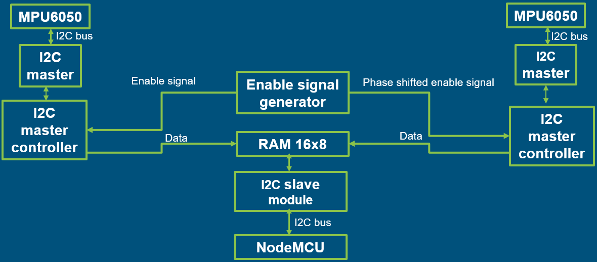
Figure1:System overview of FPGA based multi I2C controller
The system consist of several components
- I2C master
- I2C master controller
- Enable signal generator
- 16 x 8 RAM
- I2C slave module
- NodeMCU
- MPU6050 for testing
I2C master
I2C master is a VHDL module which was responsible for generating required I2C bit patterns. It uses a state machine to conduct read and write operations. The developed system uses two I2C masters to control two MPU6050 sensors. This module contains a generic input called “DEVICE” to hold the slave device address that it is communicating. Every state in state machine gets executed only if the signal called “TIC” is high. TIC is running as three times as the I2C bus speed. To transmit a bit it uses three states in the three states the SCL line gets pull down, pull up and then again put down so the TIC frequency gets divided by three and generates the SCL signal.
I2C master controller
This module is responsible for controlling the I2C master and sends the register addresses and the values that needs to be read and set. This module also uses a state machine to generate its main functionality. Furthermore it contains a pin called “Completed” that get toggles after reading all the 14 registers from the MPU6050 sensor. This pin is connected to a BitScope to measure the maximum achievable data rates. The reading cycle continues only if the signal from the enable signal generator is high.
Enable signal generator
This component is connected to the I2C master controller, and sends enable signals to the two I2C master controllers with a phase difference. Furthermore it uses a variable called count that gets incremented every master clock cycle, when it reaches a specified value a pin get toggled. This generates the required frequency signal using the master clock. Inverse of that is given to another pin so there will be a phase difference in both signals.
RAM 16 x 8
The RAM holds the data read from the MPU6050 and it is connected to the I2C slave module. Even if the MPU6050 only have 14 registers available 16×8 RAM was used to reduce synthesize warnings. RAM allowed to arrange the data in order.
I2C slave module
This module communicates with external I2C master device such as a NodeMCU and sends data that stored in the RAM. Five processes are running in the I2C slave module. Those are S_RSY,START_BIT,STOP_BIT,RD_S_DELAY, OTO. S_RSY is responsible for assigning the SCL and SDA signals from master to internal signal so those can be decoded. START_BIT and STOP_BIT processes generates the start and stop conditions based on the SCL, SDA signal and assigns to internal signal to use in the OTO process. OTO process runs the main functionality of the I2C slave and contains a state machine.
NodeMCU
NodeMCU uses the wire.h library to communicate with the I2C slave module and wire.h library allows to generate I2C speeds of 100 kbit/s and 400kbit/s. Pullup configuration was used in the ucf file for the connections between NodeMCU and FPGA board.
MPU6050
MPU6050 is a MEMS accelerometer and a gyroscope within a single chip and capable of reading temperature also. It contains 16 bit analog to digital conversion hardware for each channel. I2C protocol requires terminating resistors or pull up resistors but the used MPU6050 sensors contained those so the sensors were directly connected to the FPGA board.
Hardware
The Basys 2 FPGA board was used to develop the multi I2C controller which contains a Spartan 3E-100 CP 132 FPGA chip. BitScope was used to monitor the data rates that can be achievable. MPU6050 is the I2C sensor module that used for testing.
Results
Using only one MPU6050 the maximum achievable data rate was 209.9 Hz. Even if the sensors were enabled at speeds such as 4 kHz maximum achievable data rate was 209.9 Hz. Obtained readings are attached in the following table.
| Enable signal frequency | Data rate |
| 4 kHz | 209.9 Hz |
| 2 kHz | 209.8 Hz |
| 1 hHz | 209.9 Hz |
| 200 Hz | 198 Hz |
Using two MPU6050 sensors that gets enabled one after another it was possible to achieve 402.2Hz. This is shown in Figure 2. So it is clear that the multi I2C controller was success.
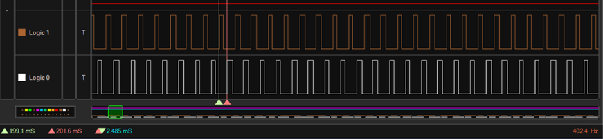
Figure2: Data rate was doubled running two sensors and 402.4 Hz achieved
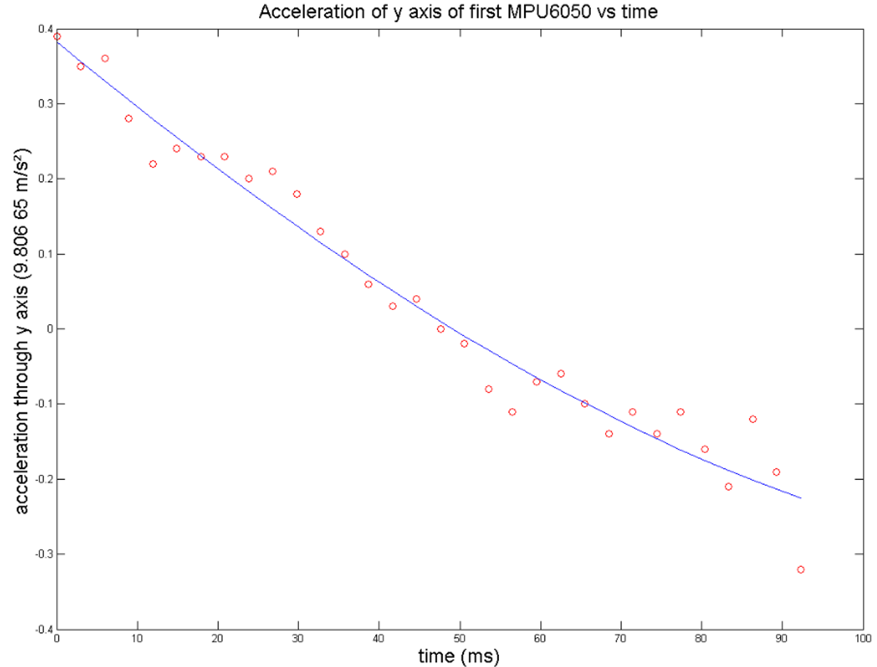
Figure 3: Graph generated using one MPU6050
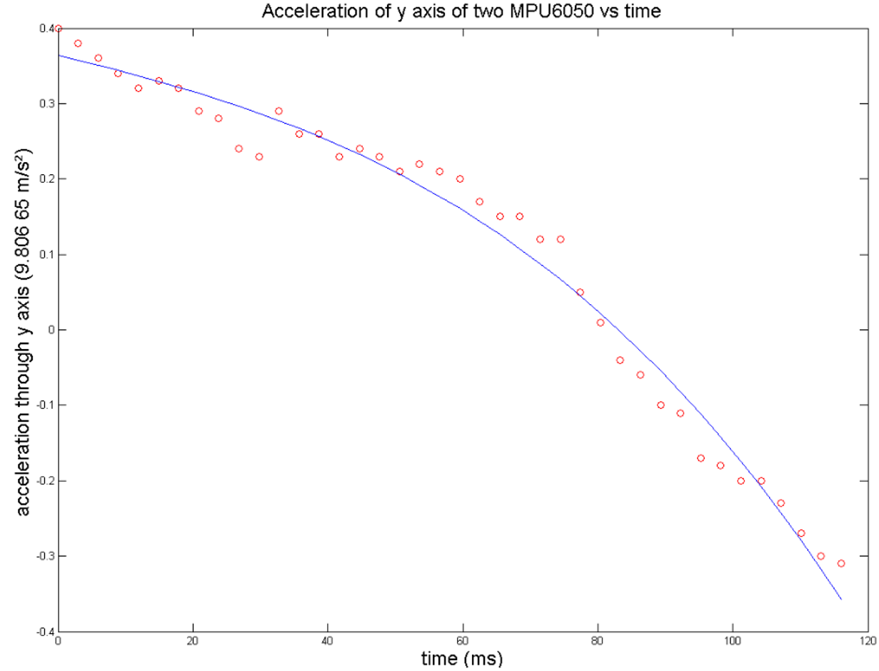
Figure 4: Graph generated using data from two MPU6050s
Figure 3 shows a graphs obtained using reading from a single MPU6050 and Figure 4 shows a graph obtained from running two MPU6050s. It can be observed that when running two MPU6050 it gives much more smoother results.
Future developments
System can be developed to handle more and more devices but these devices need to get activated with different phase shifts such as 900 so. At the moment system only handles MPU6050 and it can be developed to handle more sensors such as ADXL435. At the moment multi I2C controller is not capable of identifying sensors individually so it is difficult to apply calibration data to individual sensor as it is unique to each sensor. Extra memory available in the RAM can be used for this purpose and give a id for each sensor when it writes data to RAM. So from the NodeMCU it is possible to identify from which sensor these data are from.