In this tutorial a LED blinking program will be written without using built in libraries.
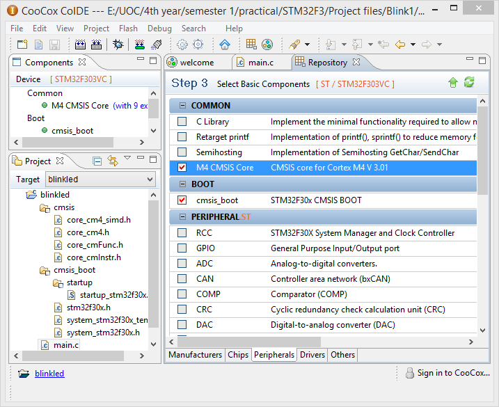
First create a new project as discussed in tutorial 2 and select M4 CMSIS Core and cmsis_boot form repository.
CMSIS libraries for STM32F3
Now double click on main.c and enter the following code.
#include <stm32f30x.h>

int main(void)
{
volatile unsigned int i =0;
RCC -> AHBENR |= 1 << 21; //Enable CLK for port E
GPIOE->MODER |= 1 << 26; // Enable PORTC pin 8 as digital output
GPIOE -> ODR |= 1<<13; // Turn GPIOC Pin 8 ON

while(1)
{
for (i = 0; i < 1000000; ++i) ; GPIOE -> ODR |= 1<<13; // Turn GPIOC Pin 8 ON
for (i = 0; i < 1000000; ++i) ; GPIOE -> ODR &= ~(1<<13); // Turn GPIOC Pin 8 ON
}
}
Understanding Code
Following line includes library related to this STM32F303VC chip. This file contains address of each and every register in this chip. By adding this header file, program includes all the information about addresses in chip into our program. If not one will have write program from scratch by redefining address in chip. This setting header file is available on STMicroelectronics website and anybody can download and use it. You can see what’s in this header file by clicking on file name in the program while press and holding CTRL button in keyboard. It will open the file in another tab.
#include <stm32f30x.h>
As in normal C program main method carries body program and it will be executed first at runtime.
int main(void)
{
}
Next line of the program is a variable defined to use in for loop. Use of this for loop will be discussed in later part of this tutorial.
volatile unsigned int i =0;
From now on everything discuss will be regarding STM32F303VC chip. Registers are specific to this chip only. But thinking logic is same for all ARM chips. So if you are using different chip just follow the procedure and try to understand you chip using datasheet and write program according to it. Here we are not using built in libraries in repository and just call into registers directly.
Next line in the program, enables clock for port E.
RCC -> AHBENR |= 1 << 21; //Enable CLK for port E
Reset and clock control (RCC) structure handle clock for different parts in the chip. As described above if you look into stm32f30x.h header file you will see following code structure there.
typedef struct
{
  __IO uint32_t CR;         /*!< RCC clock control register,                                  Address offset: 0x00 */
  __IO uint32_t CFGR;       /*!< RCC clock configuration register,                            Address offset: 0x04 */
  __IO uint32_t CIR;        /*!< RCC clock interrupt register,                                Address offset: 0x08 */
  __IO uint32_t APB2RSTR;   /*!< RCC APB2 peripheral reset register,                          Address offset: 0x0C */
  __IO uint32_t APB1RSTR;   /*!< RCC APB1 peripheral reset register,                          Address offset: 0x10 */
  __IO uint32_t AHBENR;     /*!< RCC AHB peripheral clock register,                           Address offset: 0x14 */
  __IO uint32_t APB2ENR;    /*!< RCC APB2 peripheral clock enable register,                   Address offset: 0x18 */
  __IO uint32_t APB1ENR;    /*!< RCC APB1 peripheral clock enable register,                   Address offset: 0x1C */
  __IO uint32_t BDCR;       /*!< RCC Backup domain control register,                          Address offset: 0x20 */
  __IO uint32_t CSR;        /*!< RCC clock control & status register,                         Address offset: 0x24 */
  __IO uint32_t AHBRSTR;    /*!< RCC AHB peripheral reset register,                           Address offset: 0x28 */
  __IO uint32_t CFGR2;      /*!< RCC clock configuration register 2,                          Address offset: 0x2C */
  __IO uint32_t CFGR3;      /*!< RCC clock configuration register 3,                          Address offset: 0x30 */
} RCC_TypeDef;

#define RCC                 ((RCC_TypeDef *) RCC_BASE)
As you can see all these register are predefined here. Now let’s understand how to program chip by looking at datasheet. The on board LEDs are connected port E (See tutorial one or datasheet). Our target in this tutorial is blinking LD10 led connected to pin 13 in PORT E.
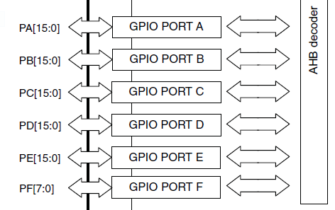
GPIO Hardware Layout
Above figure in datasheet hardware layout shows that GPIO PORT E is connected to AHP decoder which is in AHB peripheral. So one should call RCC AHB peripheral clock register to enable clock for GPIO. AHB enable register is defined as AHBENR (see above RCC typedef). Now let’s look at AHBENR register in datasheet.
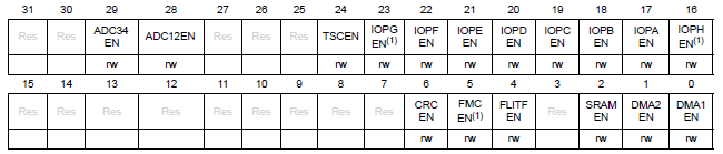
AHBENR register
Bit 21 IOPEEN: I/O port E clock enable (STM32F303xB/C and STM32F358xC devices only)
Set and cleared by software.
0: I/O port E clock disabled
1: I/O port E clock enabled.
This line RCC -> AHBENR |= 1 << 21; simply write bit 1 for 21st bit to enable clock for port E.
Now next line configures pin 13 as digital output.
GPIOE->MODER |= 1 << 26; // Enable PORTE pin 13 as digital output
Again in the chip header file you will find a code snippet as follows. (All these lines are not in same place. GPIOE is in different place in file. Its better if you search though file)
typedef struct
{
  __IO uint32_t MODER;        /*!< GPIO port mode register,                                  Address offset: 0x00 */
  __IO uint16_t OTYPER;       /*!< GPIO port output type register,                           Address offset: 0x04 */
  uint16_t RESERVED0;         /*!< Reserved,                                                                 0x06 */
  __IO uint32_t OSPEEDR;      /*!< GPIO port output speed register,                          Address offset: 0x08 */
  __IO uint32_t PUPDR;        /*!< GPIO port pull-up/pull-down register,                     Address offset: 0x0C */
  __IO uint16_t IDR;          /*!< GPIO port input data register,                            Address offset: 0x10 */
  uint16_t RESERVED1;         /*!< Reserved,                                                                 0x12 */
  __IO uint16_t ODR;          /*!< GPIO port output data register,                           Address offset: 0x14 */
  uint16_t RESERVED2;         /*!< Reserved,                                                                 0x16 */
  __IO uint32_t BSRR;         /*!< GPIO port bit set/reset registerBSRR,                     Address offset: 0x18 */
  __IO uint32_t LCKR;         /*!< GPIO port configuration lock register,                    Address offset: 0x1C */
  __IO uint32_t AFR[2];       /*!< GPIO alternate function low register,                Address offset: 0x20-0x24 */
  __IO uint16_t BRR;          /*!< GPIO bit reset register,                                  Address offset: 0x28 */
  uint16_t RESERVED3;         /*!< Reserved,                                                                 0x2A */
}GPIO_TypeDef;
#define GPIOE               ((GPIO_TypeDef *) GPIOE_BASE)
As you can see again this GPIOE has different registers to handle its task. In our coding we have called MODER Register to set pin mode. In datasheet you will find MODER register as follows.
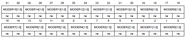
MODER register
According to this register definition two consecutive bits handles the mode of each pin. Pin 13 is handled by 26th and 27th bits of register. Depending on two bit configuration following settings will be applied to the pin.
- 00: Input mode (reset state)
- 01: General purpose output mode
- 10: Alternate function mode
- 11: Analog mode
Our code in program (GPIOE->MODER |= 1 << 26) writes bit one to 26th bit leaving 27th bit 0 which makes the pin 13 output.
The next line write bit 1 for pin 13 which make it to give output logic high voltage. ODR register also in same structure as MODER.
GPIOE -> ODR |= 1<<13; // Turn GPIOE Pin 13 ON
Next lines in the code are enclosed using infinite while loop which runs forever as long as power is supplied. Within this while loop there are two lines and which set output bit of pin 13 high and low. Operation of these two lines are discussed in above paragraph.
for (i = 0; i < 1000000; ++i) ;
Task of this long for loop is generate a delay. There is no STM32F3 chip function to make delay. So simplest way of making delay is making core busy for a while by going through a long loop.
Finally click on build button on tool bar to compile and then click on flash button to download into micro controller.
Watch the video below.