In this tutorial pulse width modulation application was implemented using STM32F3 Discovery board.
PWM is a modulation technique that change width of a pulse. This width depend on modulator signal information. Therefor this technique can be used to encode information into a signal. And also it uses as a technique of controlling power. Here it is used to create LED dimming effect.
First a new project was created and RCC, GPIO, TIM, M4 CMSIS Core, cmsis_boot libraries were included into project.
Then following code was entered in IDE.
#include <stm32f30x.h>
#include <stm32f30x_rcc.h>
#include <stm32f30x_gpio.h>
#include "stm32f30x_tim.h"

/* #function prototypes goes here ---------- */
void PWM_Init(void);
void Delay(unsigned int);

int main(void)
{
	PWM_Init();

	TIM_SetCompare1(TIM4,0);

    while(1)
    {
    	unsigned char var;
    	for (var = 0; var < 50; ++var) {     		TIM_SetCompare1(TIM4, var);     		Delay(50000); 		}     	for (var = 50; var > 0; --var) {
    	    		TIM_SetCompare1(TIM4, var);
    	    		Delay(50000);
    	}
    }
}


void Delay(unsigned int n){
	unsigned int i =0;
	for ( i = 0; i < n; ++i) ;
}


void PWM_Init(void)
{
	GPIO_InitTypeDef            GPIO_InitStructure;				//structure for GPIO setup
	TIM_TimeBaseInitTypeDef     TIM_TimeBaseStructure;			//structure for TIM Time Base
	TIM_OCInitTypeDef			TIM_OCInitStructure;			//structure for TIM Output Compare

	RCC_AHBPeriphClockCmd(RCC_AHBPeriph_GPIOB, ENABLE);			//enable the AHB Peripheral Clock to use GPIOB
	RCC_APB1PeriphClockCmd(RCC_APB1Periph_TIM4, ENABLE);		//enable the TIM4 clock

	/* Pin configuration */
	GPIO_InitStructure.GPIO_Pin = GPIO_Pin_6;						GPIO_InitStructure.GPIO_Mode = GPIO_Mode_AF;
	GPIO_InitStructure.GPIO_OType = GPIO_OType_PP;
	GPIO_InitStructure.GPIO_Speed = GPIO_Speed_Level_2;
	GPIO_InitStructure.GPIO_PuPd = GPIO_PuPd_UP;
	GPIO_Init(GPIOB, &GPIO_InitStructure);
	GPIO_PinAFConfig(GPIOB, GPIO_PinSource6, GPIO_AF_2);


	TIM_TimeBaseStructure.TIM_Prescaler = 71;
	TIM_TimeBaseStructure.TIM_Period = 49;	TIM_TimeBaseStructure.TIM_CounterMode = TIM_CounterMode_Up;
	TIM_TimeBaseInit(TIM4, &TIM_TimeBaseStructure);

	TIM_OCInitStructure.TIM_OCMode = TIM_OCMode_PWM1;
	TIM_OCInitStructure.TIM_OutputState = TIM_OutputState_Enable;
	TIM_OC1Init(TIM4, &TIM_OCInitStructure);

	TIM_CtrlPWMOutputs(TIM4, ENABLE);							//enable the PWM output
	TIM_Cmd(TIM4, ENABLE);
}
Then following circuit was connected to the board.
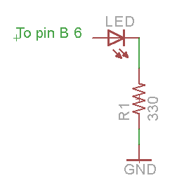
Connecting LED to PWM pin
Understanding the code
Let’s start with function PWM_Init(). This function initialize pwm function in the chip. First it is require 3 structures. GPIO structure was discussed in previous tutorials so let’s understand the function of this new structure.
TIM_TimeBaseInitTypeDef TIM_TimeBaseStructure;
TIM_OCInitTypeDef TIM_OCInitStructure;
Best way to understand is looking into header file information. Press and hold the CTRL button in key board and then click on function name. You will see several structure variables and their function as a comment in this structure TIM_TimeBaseInitTypeDef. What it basically does is, set Prescaler (devide the Tim clock), Counter mode and Period.
TIM_OCInitTypeDef structure set PWM configuration. You can see further details about this structure in header file.
The MCU on the STM32F3-Discovery board is clocked at 72Mhz and we need a 20kHz timebase (50us period)
Update_event = TIM_CLK /((PSC + 1)*(ARR + 1)*(RCR + 1))
20000 = 72000000/((71 + 1)*(49 + 1)*(0 + 1))
TIM_TimeBaseStructure.TIM_Prescaler = 71;
PSC value means that TIM register will be incremented every 1us (72000000 / (71+1) = 1000000Hz = 1us
TIM_TimeBaseStructure.TIM_Period = 49;
(ARR value – 1) create a time period of 50us (1us * 50 = 50us)
Other initialization functions has same behavior as in previously described GPIO initialization function.
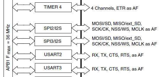
Timer 4 Peripheral Layout
As you can see in the above figure TIM4 is connected to APB1 Peripheral. Therefore RCC_APB1PeriphClockCmd function was used to enable clock for TIM4. Further details about function and suitable parameters are available in header file help.
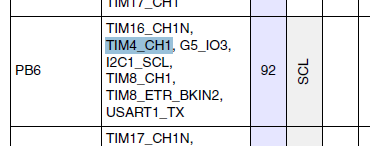
PB6 Alternative Function
According to datasheet TIM4 channel 1 is the alternative function of PB6 pin. Therefore alternative function of PB6 should initialize using GPIO_Init() to activate it. GPIO code does this in the cording.
TIM_CtrlPWMOutputs() function enable or disable the TIM peripheral Main Outputs.
TIM_Cmd () function enables or disables the specified TIM peripheral.
That’s all for PWM initialization. Now lets look at code in main function. TIM_SetCompare1() function sets the TIM4 Capture Compare1 Register value. It is used to control pulse width of signal.
Now compile the code and flash it into board and see the result.
Next PWM example shows how to control multiple PWM at same time this is an important application in robotics. Because PWM signals are used to control position of servo motors.
Example 2: Multiple PWM signals
#include <stm32f30x.h>
#include <stm32f30x_rcc.h>
#include <stm32f30x_gpio.h>
#include "stm32f30x_tim.h"

/* #function prototypes goes here*/
void PWM_Init(void);
void Delay(unsigned int);

int main(void)
{
	unsigned char LED1dc=25, LED2dc=50, LED3dc=10;

	PWM_Init();

    while(1)
    {
		TIM_SetCompare1(TIM4,(50 * LED1dc)/100);
		TIM_SetCompare2(TIM4,(50 * LED2dc)/100);
		TIM_SetCompare3(TIM4, (50 * LED3dc)/100);

		LED1dc++;
		if (LED1dc>100)
			LED1dc=0;

		LED2dc++;
		if (LED2dc>100)
			LED2dc=0;

		LED3dc++;
		if (LED3dc>100)
			LED3dc=0;

		Delay(50000);
    }
}

void Delay(unsigned int n){
	unsigned int i =0;
	for ( i = 0; i < n; ++i) ;
}

void PWM_Init(void)
{
	GPIO_InitTypeDef        	GPIO_InitStructure;			//structure for GPIO setup
	TIM_TimeBaseInitTypeDef 	TIM_TimeBaseStructure;		//structure for TIM Time Base
	TIM_OCInitTypeDef			TIM_OCInitStructure;		//structure for TIM Output Compare

	RCC_AHBPeriphClockCmd(RCC_AHBPeriph_GPIOB, ENABLE);		//enable the AHB Peripheral Clock to use GPIOB
	RCC_AHBPeriphClockCmd(RCC_AHBPeriph_GPIOD, ENABLE);		//enable the AHB Peripheral Clock to use GPIOD
	RCC_APB1PeriphClockCmd(RCC_APB1Periph_TIM4, ENABLE);	//enable the TIM4 clock

	/* Pin configuration for PB6 */
	GPIO_InitStructure.GPIO_Pin = GPIO_Pin_6;  //configure PB6 in alternate function pushpull mode
	GPIO_InitStructure.GPIO_Mode = GPIO_Mode_AF;
	GPIO_InitStructure.GPIO_OType = GPIO_OType_PP;
	GPIO_InitStructure.GPIO_Speed = GPIO_Speed_Level_2;
	GPIO_InitStructure.GPIO_PuPd = GPIO_PuPd_UP;
	GPIO_Init(GPIOB, &GPIO_InitStructure);
	GPIO_PinAFConfig(GPIOB, GPIO_PinSource6, GPIO_AF_2);	//connect the pin to the desired peripherals' Alternate Function (AF) - TIM4 (GPIO_AF_2)

	/* Pin configuration for PD13 and PD14 */
    GPIO_InitStructure.GPIO_Pin = GPIO_Pin_13 | GPIO_Pin_14;//configure PB13 and PD14 in alternate function pushpull mode
    GPIO_InitStructure.GPIO_Mode = GPIO_Mode_AF;
    GPIO_InitStructure.GPIO_OType = GPIO_OType_PP;
    GPIO_InitStructure.GPIO_Speed = GPIO_Speed_Level_2;
    GPIO_InitStructure.GPIO_PuPd = GPIO_PuPd_UP;
    GPIO_Init(GPIOD, &GPIO_InitStructure);
	GPIO_PinAFConfig(GPIOD, GPIO_PinSource13, GPIO_AF_2);	//connect the pin to the desired peripherals' Alternate Function (AF) - TIM4 (GPIO_AF_2)
	GPIO_PinAFConfig(GPIOD, GPIO_PinSource14, GPIO_AF_2);	//connect the pin to the desired peripherals' Alternate Function (AF) - TIM4 (GPIO_AF_2)

    TIM_TimeBaseStructure.TIM_Prescaler = 71;  				//PSC value; meanse that TIM register will be incremented every 1us (72000000 / (71+1) = 1000000Hz = 1us
    TIM_TimeBaseStructure.TIM_Period = 49;                 	//ARR value - 1; create a time period of 50us (1us * 50 = 50us)
    TIM_TimeBaseStructure.TIM_CounterMode = TIM_CounterMode_Up;
    TIM_TimeBaseInit(TIM4, &TIM_TimeBaseStructure);

	/* Output Control (OC) configuration - PWM1 Mode configuration: Channel1 */
    TIM_OCInitStructure.TIM_OCMode = TIM_OCMode_PWM1;		//configure the PWM
    TIM_OCInitStructure.TIM_OutputState = TIM_OutputState_Enable;

    TIM_OC1Init(TIM4, &TIM_OCInitStructure);				//for channel 1
	TIM_OC2Init(TIM4, &TIM_OCInitStructure);				//for channel 2
	TIM_OC3Init(TIM4, &TIM_OCInitStructure);				//for channel 3

	TIM_CtrlPWMOutputs(TIM4, ENABLE);						//enable the PWM output
	TIM_Cmd(TIM4, ENABLE);									//enable TIM4
}
In this case also LEDs are connected pins which are defined to use alternative function. Compile the code and see the result.
Watch the video below