Introduction
Persistence of Vision (POV) Wands is a way to create long light displays. The wand consists of a single row of LED’s controlled by an ATMEL 328 Micro controls. When the wand is turn on the Leds are lighting on randomly, but if you move it quickly left and right, you will see Message. Twenty LED bulbs are in a single line. The message display the LED patent dribbling speed tally to the moving speed the message is displayed well otherwise can read the message.
overview
The project undertook was a motion in display the message in wand .The At-mega 328 micro-controller was used in this project to generate binary patterns of the respective keys. The generated binary patterns are fed into the wand LED of a PC.
The result of this project is a valuable device that enables easy use of the PC. With one sweep of the hand you can move through a page or a presentation slide giving you much more freedom.
objectives
Objectives of this project are get experiences and good knowledge about the micro-controller and its applications (How the PIC is program, how it connect to the other electric devices.). Can improve skills of making circuit and get the experience about the PCB design.
organization of the report
Although many designs have been made to LED through a micro-controller to the PC, designs which require the use of the all the ports was almost possible to find. Therefore the design process and the programming had to be done beginning from scratch.
The main targets faced in this project were creating the wand which is display the message in when the wand is moving left to right. Therefore certain commands had to be programmed to the micro-controller and a suitable communication program must be executed at the start up.
The material and the design methods are explained in the chapter 2. The design and construction are explained in the chapter 2.
Materials and methods
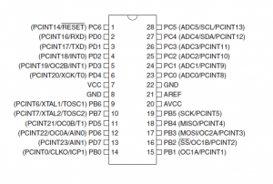
When Building the schematic diagram, Based on the LED, as it is a p-n junction diode. As the other diodes current flow through a LED is from p side (anode) to the n side (cathode) not in reverse direction. LED will begin to emit the light when the external voltage is exceeded than the potential barrier of the diode. AT MEGA 328 IC.
I/O and Package – 23 Programmable I/O Lines, Operating Voltage: 1.8 to 5.5V,
METHOD
This instrument using delay timing give the current to the each and every led and lighting it .
Design and construction
Orcad 16.5 software was used to design the all the hardware parts of this project. First of the complete schematic diagrams of the hardware was drawn. Then components were supplied and they were checked using the bread board and power supply. The beginning of the project, 12 V was taken as the power supply. But after checking LED’s with pin touch was used. After checking all the components suitable components were chosen. Then the hardware was separated to a suitable way to construct. The PCB layouts were designed also using the Orcad software. This project is basically consisting of four hardware parts.
- The part consists of LED’s.
Procedure- BLOCK DIAGRAM
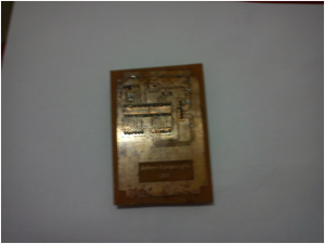
PCB layer-out
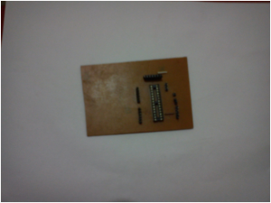
The bottom layer of the circuit was basically used for the necessary components needed to run the Atmega 328. It acts as a custom board for this device. The wire outs for the top layer and the LED port were left through connectors.
Components
Components used to construct the mother board
| Component | Description | Quantity |
| Atmeg 328 micro controller | 1 | |
| Resistors | 100 ohm | 20 |
| Connecters | D-SUB 9 female serial | 1 |
| 2 pin | 1 | |
| 4 pin | 1 | |
| 6 pin | 2 | |
| 6 pin | 2 | |
| 3 pin | 1 | |
| 1 | ||
| LED | Normal | 20 |
| Diode | 1 | |
| Switchers | 6 mm | 1 |
Table 1 –
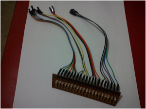
The part consists of LED’s
The part consists of PCB with component
The part consists of PCB
Components used to construct the part consists of LEDs.
| Component | Description | Quantity |
| Connecters | 1 pin | 7 |
| LED | ||
| Read | 2 | |
Table 2 –
APPENDIX A
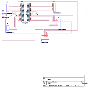
Figure 14: Schematic diagram of the Persistence of Vision Wands used (bottom layer)
Finale product
Result and analysis
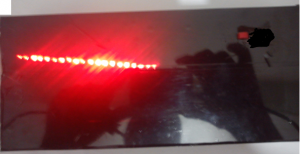
The all hardware parts of the project are worked. But the. Therefore the micro controller was programmed using the bread board of the lab .After connecting all the parts the final product were taken. When the 6 V (to the LED’s) and 5 V (to the bread board) power, supply to the device it will automatically emit read colors and 5 V supply to the potentiometer the brightness of blue LED not vary manually. The images in below are the photograph of the final product.
Discussion and conclusion
The main problem regarding to this project is micro controller destroyed easily.
The light beams of the LED’s were not sufficient red the message to day time. 20 LED’s were used and same circuit was made four times before finding the better way.
PCB designing three pcbboard were wasted to this one because of removing the stile the some of path removing that the major issue in the project
Future enhancements for the device
World of electronics holds many possibilities for the creative mind. Thus it is possible to enhance this device with many other added features. Or it could also be used for some other project as a basic component.
One idea is to enhance this to have more easy that could detect many other hand gestures. For example you could implement it to detect the hand making a any motion bicycle rime used to display message or ceiling fan. The direction of the motion could also be used to implement sending messages and wind turbine blades to connect the wand and advertising the messages to night.
This would let the user move freely. Of course a receiver must be placed to relay the signal.
The theory of this can be used in other projects as well. Ports are given input and output to with delay time.
The initializing process of the PCB can also be emulated if you use higher oscillator frequencies. Since the Atmega 328 only supports up to 40 MHz, Atmega 32or 168 other similar product that runs in very high speeds can be used.
Reference
http://hlt.media.mit.edu/wiki/pmwiki.php?n=Main.AVRProgrammingAdvanced
http://site.gravitech.us/Arduino/NANO30/ATMEGA328datasheet.pdf
